


SEMICON India 2025: Announcements, Deals and What India’s Semiconductor Ecosystem Gains
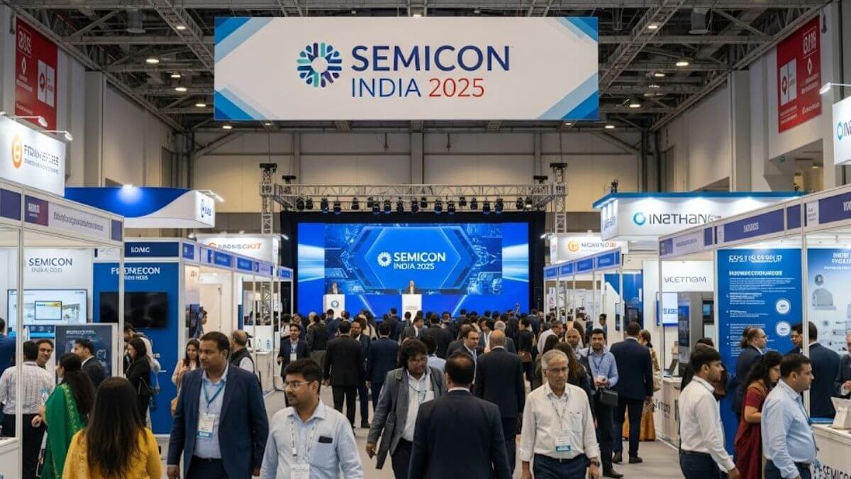
SEMICON India 2025 did more than showcase tools and panels, it turned policy intent into tangible pledges, supplier commitments and capability-building initiatives that could rewrite India’s semiconductor roadmap. The three-day event at Yashobhoomi surfaced a cluster of announcements that matter not as standalone headlines but because together they reduce execution risk, shorten supply chains and seed a domestic value chain that extends from design to packaging. Below is a focused, reporter-style coverage of the major announcements, what they concretely mean, and who benefits.
The headlines that moved the needle
The most visible financial commitment was a new deep-tech investment alliance, announced with roughly US$1 billion in initial capital commitments aimed at deep-tech ventures including semiconductors, materials and advanced packaging. This kind of upfront, patient capital addresses one of the oldest bottlenecks for chip-scale startups: long gestation, capital intensity and limited local funding for risky deep-tech.
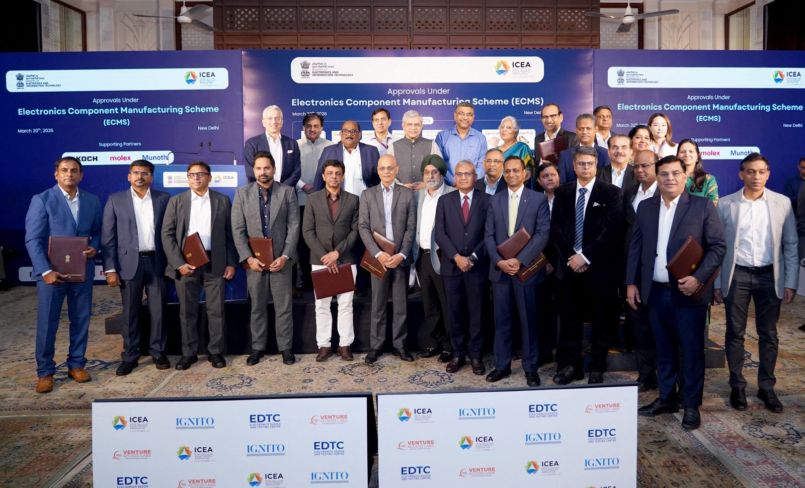
A major industry MoU that surfaced at the event was between Tata Electronics and Merck Electronics, intended to strengthen semiconductor materials, packaging and sub-fab capabilities for Tata’s planned Dholera fab and associated ATMP (assembly, test, packaging) requirements. The partnership signals that domestic fab developers are locking in upstream suppliers, a crucial step to reduce import dependence for specialty chemicals and materials.
India also used the forum to showcase indigenous design progress: the unveiling of the Vikram 32-bit processor underscored progress in local chip design and IP development, a symbolic and practical milestone for the “design → manufacture” strategy. Domestic IP creates higher-value capture opportunities beyond simple assembly.
Global supply-chain players showed up too. ASML’s senior leadership and other tier-one equipment firms publicly committed engagement and knowledge exchange; their presence is important for standards alignment, future technology transfer discussions, and for signalling that vendors are ready to support India’s ambitions.
Finally, equipment firms and integrators are already staking operational footprints: for example, Tokyo Electron announced plans to establish local offices to support Dholera and other projects, a sign that suppliers are preparing service and sales networks on the ground. That kind of local presence shortens lead times and elevates reliability for new fabs.
Why these announcements matter, concrete implications
- Capital availability meets real needs. The $1B deep-tech alliance does more than signal investor interest; it provides a form of long-term funding that matches the timelines startups and materials vendors require. Instead of one-off grants, patient capital can underwrite R&D-heavy, capital-intensive product cycles (resists, substrates, packaging tech) that are prerequisites for a resilient semiconductor stack.
- Supply-chain de-risking through upstream tie-ups. MoUs such as Tata–Merck mean fabs can negotiate for guaranteed supplies or local sourcing pathways for specialty chemicals and materials, mitigating two major project risks: long procurement cycles and supply shocks. This materially lowers the operational risk of greenfield fabs.
- Design credibility fuels higher value capture. Showcasing indigenous chips (Vikram) signals that India is investing in IP, not just assembly. Local design capabilities increase the opportunity to retain value domestically, from silicon to software integration, and to spawn startups in EDA tools, verification IP and application-specific chiplets.
- Vendor commitment = faster time-to-market. When equipment leaders publicly engage and set up local functions, procurement timelines shorten and service quality improves. This matter-of-factly raises the odds that early fabs achieve competitive yields faster, a crucial commercial metric.
- Skilling and operational readiness start getting attention. The visible push for academic and vocational tie-ups at SEMICON responds to a fundamental truth: fabs need more than capex, they need trained operators, tool engineers and metrology specialists. Announcements around skilling create a stage for vocational pipelines that will be essential during ramp-up. (Event programme and downstream initiatives highlight these tie-ups.)
Who benefits and how
Investors and PE: Short-term opportunities are in materials, packaging and ATMP integrators; mid-term upside sits with IP, EDA tools and materials startups that the new investment vehicles will incubate. The combination of private capital and policy clarity reduces execution risk and improves the investment case.
OEMs and equipment vendors: Early localisation (service hubs, training centres, spare-parts depots) captures after-sales revenue and builds stickiness; those who commit early will be preferred partners for new fabs.
Indian corporates & fab developers: Locking strategic MoUs with global materials suppliers de-risks timelines and procurement an advantage in competitive siting and financing rounds.
MSMEs & ancillaries: Construction, HVAC/cleanroom services, precision machining, chemical intermediates, and logistics firms stand to see near-term demand. MSMEs should immediately map capabilities against ATMP and fab supplier checklists and pursue vendor certification paths.
Academia & skilling providers: There’s an urgent demand to co-design short, job-aligned credential programmes for cleanroom technicians, metrology experts and equipment engineers a clear monetizable opportunity.
Practical next steps (for organisations covering or acting on these announcements)
- Track procurement milestones rather than MoUs, supplier contracts and equipment purchase orders will be the earliest verifiable signs of execution.
- MSMEs should get vendor-ready: quality certifications, cleanroom-friendly processes and traceable quality systems.
- Investors should build thesis frameworks focused on suppliers, packaging and materials where local demand is immediate.
- Policy makers must now convert momentum into execution: expedite clearances, refine incentives for supplier localisation, and fast-track vocational pipelines.
The caveat
SEMICON India 2025 created momentum, but the heavy lifting remains. Fabs are multi-year projects dependent on global suppliers (some of which are not immediately localisable), and workforce scale-up will take time. Success will be measured by procurement milestones, construction progress, equipment installations and ramped yields, not by announcements alone.
SEMICON India 2025 was a credible shift from aspiration to pipeline: capital pledges, supplier MoUs, vendor commitments and design showcase now give India a practical shot at building an ecosystem that goes beyond assembly. For journalists and corporate communicators covering this space, the story has moved from “will India” to “how fast and how well” and the next 18–36 months will determine whether the chips moment becomes a durable industrial transformation or a missed window. Those who map capability gaps, move decisively on supplier relationships and convert MoUs into contracts will be the first to convert visibility into value.