



Semicon 2.0 and India’s New Mobile Manufacturing Push: The Next Chapter of India’s Electronics Ambition
India’s journey from being one of the world’s largest electronics importers to becoming a major manufacturing destination has entered a new phase. In a landmark decision on Wednesday, the Union Cabinet has approved Semicon 2.0 with an outlay of ₹1.27 lakh crore and a new Mobile Phone Manufacturing Scheme (MPMS) worth ₹62,500 crore, signalling the government’s intent to build a complete electronics and semiconductor ecosystem rather than merely assembling products.
For India’s SMEs, startups, component manufacturers, precision engineering firms, logistics providers, chemical suppliers and technology companies, the announcement is far more than another incentive scheme. It represents the creation of an entirely new industrial ecosystem that could reshape manufacturing, exports and technology leadership over the next decade.
Why Was Semicon 2.0 Needed?
Semiconductors have become the foundation of the modern economy.
From smartphones and automobiles to industrial automation, medical devices, defence systems, artificial intelligence, telecommunications and consumer electronics, almost every technology product today depends on semiconductor chips.
The COVID-19 pandemic exposed the vulnerabilities of global supply chains when chip shortages disrupted production across industries worldwide. Countries quickly realised that semiconductors were not merely commercial products, but strategic assets linked to economic security, technological competitiveness and national resilience.
India, despite being one of the world’s fastest-growing electronics markets, remained heavily dependent on imported chips. While the country emerged as a major mobile phone manufacturing hub, much of the high-value semiconductor ecosystem remained concentrated in countries such as Taiwan, South Korea, China, Japan and the United States.
The first phase of India’s semiconductor strategy, known as ISM 1.0 (India Semiconductor Mission), was launched to address this gap. Semicon 2.0 builds upon that foundation with a broader objective: creating a complete semiconductor value chain within India.
The government’s vision is clear. India should not merely manufacture electronics products; it should participate in the high-value activities of chip design, fabrication, packaging, research, materials and equipment manufacturing.
Understanding the Six Pillars of Semicon 2.0
The most significant aspect of Semicon 2.0 is its ecosystem-based approach. Unlike traditional incentive schemes that focus solely on manufacturing, the programme targets six interconnected pillars.
Design and Intellectual Property: India already has a strong semiconductor design presence. Many global semiconductor companies operate design centres in Bengaluru, Hyderabad, Noida and Pune.
Under ISM 1.0, 105 startups and MSMEs received access to industry-standard Electronic Design Automation (EDA) tools, while 24 semiconductor design projects received financial support.
Semicon 2.0 aims to deepen this ecosystem by encouraging indigenous chip design, system architecture development and intellectual property creation.
This is particularly important because the highest value creation in semiconductors often occurs at the design stage rather than manufacturing alone.
Machines, Materials and Chemicals: One of the most overlooked parts of semiconductor manufacturing is the extensive ecosystem of ultra-pure chemicals, specialty gases, advanced materials and precision manufacturing equipment.
A modern semiconductor fab requires thousands of specialized inputs.
Semicon 2.0 will incentivize companies involved in:
- Semiconductor-grade chemicals
- Specialty gases
- Silicon wafers
- Manufacturing equipment
- Precision engineering systems
This presents a major opportunity for India’s MSMEs operating in chemicals, engineering, industrial manufacturing and advanced materials.
More Semiconductor Fabs: India’s first semiconductor fabrication facility is expected to become operational by 2028.
Semicon 2.0 seeks to attract additional investments across: Silicon fabs, compound semiconductor fabs, discrete semiconductor fabs, display fabs.
The objective is to increase domestic manufacturing capacity and reduce import dependence over time.
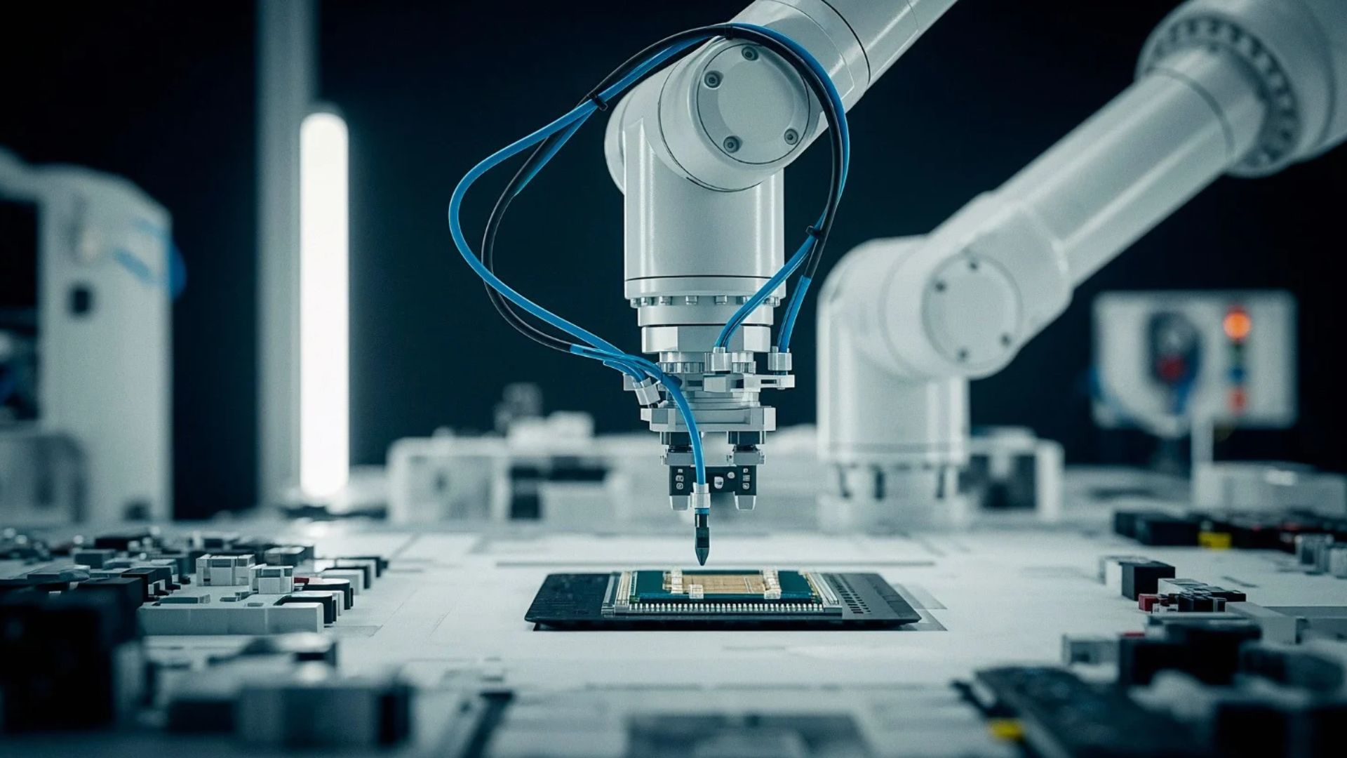
Expanding the ATMP and OSAT Ecosystem: Assembly, Testing, Marking and Packaging (ATMP) and Outsourced Semiconductor Assembly and Test (OSAT) facilities are critical parts of the semiconductor supply chain.
These facilities package semiconductor chips before they are integrated into final products. India has already attracted significant investments in this segment and is increasingly being viewed as an alternative manufacturing destination.
The government now aims to bring advanced packaging technologies to India, creating new opportunities for component suppliers and manufacturing SMEs.
Research and Development: The first wave of semiconductor manufacturing in India focuses primarily on 28nm to 110nm technology nodes.
Semicon 2.0 aims to support research into advanced semiconductor technologies and next-generation nodes through partnerships with domestic and international research institutions.
This is essential if India wants to move beyond manufacturing into technology leadership.
Talent Development: Perhaps one of the most important pillars is human capital.
So far 315 universities are participating in semiconductor training programmes & nearly 68,000 students have been trained using advanced chip design tools.
The next phase will deepen industry-academia collaboration and develop specialized skills in: Chip design, Clean-room operations, Fab management, Advanced manufacturing, Packaging technologies.
What Has India Achieved Under ISM 1.0?
The government’s decision to launch Semicon 2.0 is rooted in the significant momentum generated under the first phase of the India Semiconductor Mission (ISM 1.0). Over the past few years, India has established a credible presence in the global semiconductor ecosystem.
So far, 12 semiconductor manufacturing projects have been approved with a cumulative investment exceeding ₹1.64 lakh crore, including a silicon fab, a silicon carbide fab, an integrated Gallium Nitride (GaN) Micro LED display fab, and nine semiconductor packaging and assembly facilities. Importantly, the transition from policy to production has already begun, with Micron Technology, Kaynes Technology and CG Semi commencing commercial operations, while another facility is expected to become operational in 2026.
Beyond manufacturing, ISM 1.0 has also laid the foundation for a domestic semiconductor design ecosystem. More than 105 startups and MSMEs have been provided access to industry-standard Electronic Design Automation (EDA) tools, enabling them to develop semiconductor solutions for applications ranging from artificial intelligence, satellite communications and drones to IoT devices, telecom equipment and smart metering systems. This progress signals a strategic shift in India’s technology landscape from being primarily a software and services powerhouse to gradually building capabilities in high-value hardware innovation, semiconductor intellectual property and advanced electronics design.
The Mobile Manufacturing Scheme: Strengthening India’s Electronics Success Story
Alongside Semicon 2.0, the Cabinet approved the Mobile Phone Manufacturing Scheme (MPMS) with an outlay of ₹62,500 crore.
The move follows the successful conclusion of the Production Linked Incentive (PLI) scheme for large-scale electronics manufacturing.
The numbers explain why a successor scheme became necessary.
Since FY2014-15: Electronics manufacturing has grown 7 times
- Electronics exports have grown 11 times
- India has become the world’s second-largest mobile phone manufacturer by volume
- 99.2% of mobile phones sold in India are now manufactured domestically
Most notably, smartphones emerged as India’s largest exported product category in 2025, surpassing traditional export leaders such as diesel fuel and cut diamonds.
Under MPMS, manufacturers will receive incentives ranging from 2.25% to 5% on eligible sales, with additional incentives linked to domestic sourcing and indigenous product design.
The scheme aims to generate mobile phone production worth approximately ₹39 lakh crore, significant export growth and around 60,000 direct jobs over five years.
What Does This Mean for SMEs?
The biggest beneficiaries may not be semiconductor giants alone.
Every semiconductor fab requires hundreds of suppliers providing chemicals, specialty materials, precision components, logistics services, clean-room equipment, automation systems, industrial software and engineering solutions.
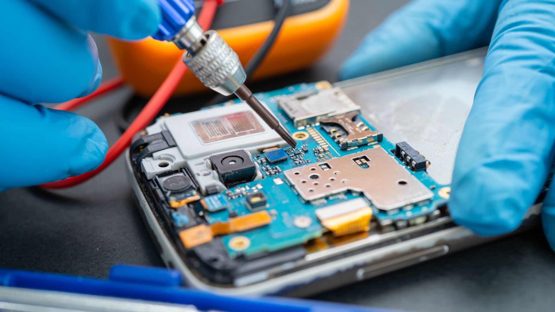
Similarly, the expansion of mobile manufacturing creates opportunities across electronic components, packaging, industrial automation, testing equipment, precision engineering, warehousing and logistics, design services.
A Defining Industrial Policy Moment
Semicon 2.0 is not merely an electronics programme. It is an industrial strategy aimed at positioning India within one of the most strategically important industries of the 21st century.
With over ₹1.9 lakh crore of combined government support through Semicon 2.0 and MPMS, India is attempting to build an end-to-end ecosystem that spans design, fabrication, packaging, materials, research and talent.
If executed successfully, the initiative could help transform India from a large electronics market into a globally competitive semiconductor and advanced manufacturing hub creating opportunities not only for large corporations but also for thousands of SMEs that will form the backbone of this emerging ecosystem.